17 January 2024

D-Algorithm

Inducing the fault in any node and propagating the fault effect from the fault site to the primary output is called D-Algorithm.

D-Algorithm uses 5-valued logic (0, 1, D, D', X).

If,

D = 1, then No Fault

D' = 0, then No Fault

D = 0, then Fault

D' = 1, then Fault


D-Algorithm Proceedure

  1. Truth Table
  2. Singular Cover
  3. Finding D-Cube with D-Intercept
  4. Propagate fault effect to PO
  5. Back-track to PI to justify


22 September 2023

MOSFETs Fabrication Process

Before know about the fabrication process of MOSFETs, we should know about the following terms SubstrateIntrinsic SemiconductorExtrinsic SemiconductorDoping, Diffusion, n-Well, nMOS, pMOS.

Substrate

Substrate is known as supporting material. It provide mechanical support, electrical isolation, and thermal dissipation. Also it has high melting point (1400°C). So upon which or within which the elements of semiconductor device are fabricated or attached.

Live example: soil is the substrate for plants. Soil act as a supporting material for plant.


Intrinsic Semiconductor

Semiconductor that are pure, in other words free from impurities are called as Intrinsic Semiconductor. That is, number of existed electrons are equal to number of holes (e = p).


Extrinsic Semiconductor

If the impurities are doped to the pure semiconductor, then it becomes Extrinsic Semiconductor.


Doping

Doping is the process of adding impurities to the intrinsic semiconductors to change their properties. Normally Trivalent and Pentavalent elements are used to dope Silicon.

If the intrinsic semiconductor is dopped with trivalent (3 electrons) impurities, then it becomes p-type semiconductor.

Trivalent materials: Boron, Gallium, Aluminium (Acceptor Impurities)

If the intrinsic semiconductor is dopped with pentavalent (5 electrons) impurities, then it becomes n-type semiconductor.

Pentavalent materials: Phosphorus, Nitrogen, Arsenic (Donor Impurities)


Diffusion

Diffusion is the net movement of anything (electron, hole, atom, ions) generally from a region of higher concentration to region of lower concentration.


n-Well

n-Well is created in p-type substrate by digging well and putting n-type material in that well.

In p-type substrate, we can make nMOS.

In n-type substrate, we can make pMOS.

But in CMOS technology, we need both nMOS and pMOS transistors to build a circuit. Both nMOS and pMOS must be fabricated on the same silicon substrate (wafer).

The wafer are mostly p-type. So, we can only make nMOS transistors in those wafers. To fabricate a pMOS transistors, we dope a selected regions of the wafer to be n-type. By digging well and fill that well by n-type material is called as n-well.


N-channel MOSFET (NMOS): In an NMOS transistor, the semiconductor channel is made of n-type material (electron-rich). The gate voltage controls the flow of electrons from the source to the drain. When a positive voltage is applied to the gate with respect to the source, it creates an electric field that attracts electrons, forming a conductive channel between the source and drain, allowing current to flow.


P-channel MOSFET (PMOS): In a PMOS transistor, the semiconductor channel is made of p-type material (hole-rich). The gate voltage controls the flow of holes from the source to the drain. When a negative voltage is applied to the gate with respect to the source, it creates an electric field that attracts holes, forming a conductive channel between the source and drain, allowing current to flow.


03 August 2023

Setup Time, Hold Time, Clock Skew, Clock Latency

"Setup Time" and "Hold Time" are important timing parameters in digital circuit design, particularly when dealing with flip-flops or registers.


Setup Time:

The setup time (Ts) is the minimum amount of time that the input signal must be stable before the active edge of the clock signal (rising or falling edge) arrives. In other words, the input data must be valid and unchanged for at least the setup time before the clock transition occurs. If the input changes too close to the clock edge, there might not be enough time for the flip-flop to properly capture the correct data.


Hold Time:

The hold time (Th) is the minimum amount of time that the input signal must remain stable after the active edge of the clock signal arrives. It ensures that the input data remains unchanged while the flip-flop captures the data. Changing the input too quickly after the clock edge can lead to data corruption or incorrect behavior.

Violations of setup and hold times can lead to timing-related issues, such as metastability, data corruption, or incorrect logic behavior. To ensure proper operation, digital designs must satisfy both setup and hold time requirements.

Designers typically analyze these timing parameters during the digital design process and perform static timing analysis to verify that these constraints are met. If the setup and hold times are not satisfied, appropriate measures must be taken, such as adjusting the clock frequency and optimizing logic paths.


Clock Skew:

The difference in the arrival time of a clock signal at two different registers, which can be caused by path length differences between two clock paths, or by using gated or rippled clocks.

Clock skew refers to the variation in arrival times of a clock signal at different points in a digital circuit. In other words, it is the difference in arrival times of the clock signal at various clocked elements, such as flip-flops, registers, and other sequential logic components. Clock skew can lead to 

  • Violations of setup and hold time requirements.
  • Reduced timing margins, which may affect performance.
  • Potential for incorrect logic behavior.


Clock Latency
:

The time taken by the clock signal to reach from clock source to the clock pin of the particular flip flop is called as clock latency.


Synchronous Clock vs. Asynchronous Clock

  • Clock is generated by Oscillator.
  • Clock is having two components :-
    • Phase (used to describe the specific location)
    • Frequency


Synchronous Clock:
Synchronous clock will have same phase and same source.


Asynchronous Clock:
Asynchronous clock will have different phase and different source.


01 August 2023

OCC - On-chip Clock Control

On-chip Clock Controller is a circuit or block to manage and control the clock signals of various on-chip components. The OCC is responsible for generating, distributing, and gating clock signals to ensure proper synchronization and timing of the chip's functional blocks.

OCC decides which clock to be probagated during Shift and Capture. Also decides how many clock pulses are required during Capture.


In Test Mode,

If SE is 1 (Shift Phase), the Scan Clock is propagated at the output of OCC.

If SE is 0 (Capture Phase), the shift register starts shifting ‘1’ and enables the Clock Gate, to allow single pulse or double pulse, depending on the type of testing. The OCC generates one clock pulse in stuck-at testing (At-speed Mode = 0) and two clock pulses in at-speed testing (At-speed Mode = 1).


PLL - Phase Locked Loop

PLL is a circuit used to generate a stable and pricised clock signal from the noisy input signal. The PLL compare the input signal with reference signal and adjust the phase and frequency of the output signal.

A PLL is a feedback control system that compares the phase of an input reference signal with a feedback signal generated by a voltage-controlled oscillator (VCO). The PLL adjusts the VCO's frequency to match the reference frequency, generating a stable clock signal.


The main components of a typical PLL are:

  • Phase Detector (PD): The phase detector compares the phase of the input reference signal (usually called the "reference signal" or "reference clock") with the phase of the feedback signal (usually called the "feedback signal" or "output clock"). It produces an error signal that represents the phase difference between the two signals.
  • Voltage-Controlled Oscillator (VCO): The VCO is an oscillator whose output frequency can be controlled by applying a voltage. The VCO generates the output signal of the PLL, which is usually called the "output clock" or "PLL output." The frequency of the VCO is controlled by the error signal from the phase detector.
  • Loop Filter: The loop filter is a low-pass filter used to filter the error signal from the phase detector and provide a smooth control voltage to the VCO. It helps stabilize the PLL and reduce jitter in the output signal.


The operation of a PLL is as follows:

  1. The phase detector continuously compares the phase of the reference signal and the feedback signal and generates an error signal.
  2. The error signal is filtered by the loop filter to obtain a smooth control voltage.
  3. The control voltage is applied to the VCO, which adjusts its output frequency to minimize the phase difference between the reference signal and the feedback signal.
  4. The output signal of the VCO becomes the feedback signal, which is fed back to the phase detector, completing the feedback loop.

31 July 2023

Pin, Pad, Port

Pin: An individual terminal or connection point on an electronic component.

Pad: A conductive area on a PCB or IC where a component's PIN is soldered for electrical connection.

Port: A group of related input or output pins in a digital system, often associated with a specific function or communication interface.


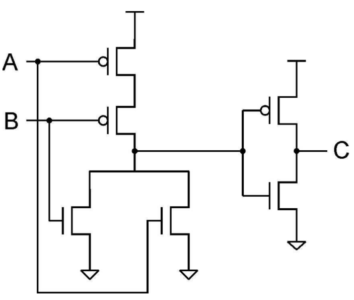
Transistor-level Diagram for Logic Gates

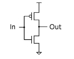
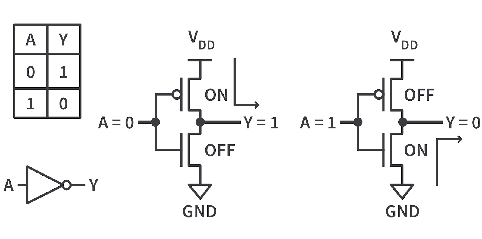
NOT Gate


AND Gate


OR Gate


NAND Gate


NOR Gate


30 July 2023

Lockup Latch

To add a half cycle delay between the two clock domain mixing in the data path or scan path to hold the data for half cycle to avoid hold violation.

Usually  Negedge D-Latch is used as Lockup Latch.

Clock Divider

Clock Divider is also called as Frequency Divider. Clock divider is a circuit, it takes a input (e.g. 100 MHz) and produce a output (e.g. 50 MHz) with lower frequency. It is used to generate different clock frequencies for different parts in the digital design.

Advantages:

1. Reduce the power consumption, in terms of slower clock.

2. Facilitate the testing and debugging, in terms of slowing down the clock.

Types

Divided by 2 Clock Divider, Divided by 3 Clock Divider, Divided by 4 Clock Divider, and etc.

Divided by 2 Clock Divider


Divided by 4 Clock Divider

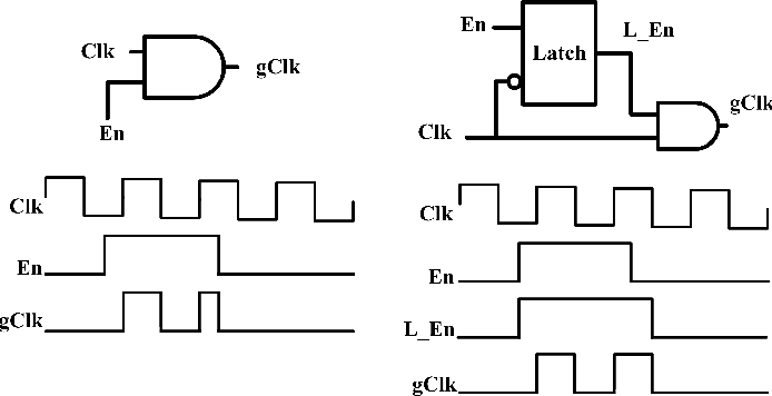
Clock Gating Circuit

Clock gaters are used to reduce the power consumption, it is a technique/methodology to turn off the clock to certain parts of the digital design when not needed.

Simple AND gate may used as clock gater. But it has some limitation, that is it will create glitches.

Hence, the circuit with Negedge Latch and AND gate is used as clock gater.


CMOS

CMOS - Complementary Metal Oxide Semiconductor

CMOS is a semiconductor technology used in most of the IC's. CMOS transistors are based on metal oxide semiconductor field effect transistor (MOSFET) technology.

CMOS circuits use a combination of p-type and n-type metal–oxide–semiconductor field-effect transistor (MOSFETs) to implement logic gates and other digital circuits. 


CMOS inverter (NOT logic gate)


MOSFET

MOSFET - Metal Oxide Semiconductor Field Effect Transistor.

MOSFET is a type of transistor used in electronic circuits for switching and amplification. It consist of metal gate electrode separated from the semiconductor channel by a thin layer of oxide, when voltage is appiled to the gate an electric field is created which controls the flow of current through the channel between the source and drain.

Source is connected to ground.

Drain is connected to load.

Gate is connected to input.


There are two main types of MOSFETs:


N-channel MOSFET (NMOS): In an NMOS transistor, the semiconductor channel is made of n-type material (electron-rich). The gate voltage controls the flow of electrons from the source to the drain. When a positive voltage is applied to the gate with respect to the source, it creates an electric field that attracts electrons, forming a conductive channel between the source and drain, allowing current to flow.


P-channel MOSFET (PMOS): In a PMOS transistor, the semiconductor channel is made of p-type material (hole-rich). The gate voltage controls the flow of holes from the source to the drain. When a negative voltage is applied to the gate with respect to the source, it creates an electric field that attracts holes, forming a conductive channel between the source and drain, allowing current to flow.


Transistor

A transistor is a semiconductor device used to amplify or switch electrical signals and power. It is one of the basic building blocks of modern electronics.

It has three terminals, namely Collector, Base, Emitter.


28 July 2023

D - Flip Flop

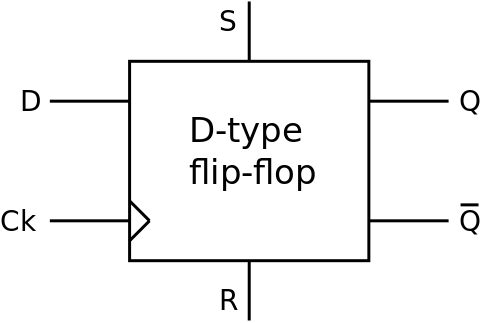
The D flip-flop is a two-input flip-flop. The inputs are the data (D) input and a clock (CLK) input. The clock is a timing pulse generated by the equipment to control operations. The D flip-flop is used to store data at a predetermined time and hold it until it is needed.


The D flip-flop has two main inputs:


  • D (Data input): This input controls the data to be stored in the flip-flop. The current value of D is transferred to the output (Q) on the rising edge (or falling edge, depending on the type of DFF) of the clock signal.
  • CLK (Clock input): The clock signal is used to control the timing of the D flip-flop. The output Q is updated based on the value of D at the specific edge of the clock signal.


The D flip-flop has two outputs:


  • Q (Output): Represents the stored data bit. It changes its state based on the input D at the rising (or falling) edge of the clock.
  • Q̅ (Complement output): Also known as the "not Q" or "Q-bar" output, it represents the complement of the Q output.


1. Schematic diagram


2. Logic diagram


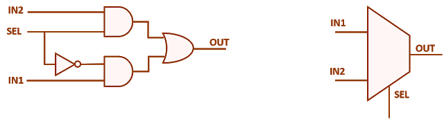
2 × 1 MUX

A 2 × 1 multiplexer consists of two inputs IN1 and IN2, one select input SEL and one output OUT.

Logic diagram and Schematic symbol


2x1 mux diagram (2).png


If SEL is 0, then IN1 will be selected.

If SEL is 1, then IN2 will be selected.


D-Algorithm

Inducing the fault in any node and propagating the fault effect from the fault site to the primary output is called D-Algorithm. D-Algorithm...