31 July 2023

Pin, Pad, Port

Pin: An individual terminal or connection point on an electronic component.

Pad: A conductive area on a PCB or IC where a component's PIN is soldered for electrical connection.

Port: A group of related input or output pins in a digital system, often associated with a specific function or communication interface.


Transistor-level Diagram for Logic Gates

NOT Gate


AND Gate


OR Gate


NAND Gate


NOR Gate


30 July 2023

Lockup Latch

To add a half cycle delay between the two clock domain mixing in the data path or scan path to hold the data for half cycle to avoid hold violation.

Usually  Negedge D-Latch is used as Lockup Latch.

Clock Divider

Clock Divider is also called as Frequency Divider. Clock divider is a circuit, it takes a input (e.g. 100 MHz) and produce a output (e.g. 50 MHz) with lower frequency. It is used to generate different clock frequencies for different parts in the digital design.

Advantages:

1. Reduce the power consumption, in terms of slower clock.

2. Facilitate the testing and debugging, in terms of slowing down the clock.

Types

Divided by 2 Clock Divider, Divided by 3 Clock Divider, Divided by 4 Clock Divider, and etc.

Divided by 2 Clock Divider


Divided by 4 Clock Divider

Clock Gating Circuit

Clock gaters are used to reduce the power consumption, it is a technique/methodology to turn off the clock to certain parts of the digital design when not needed.

Simple AND gate may used as clock gater. But it has some limitation, that is it will create glitches.

Hence, the circuit with Negedge Latch and AND gate is used as clock gater.


CMOS

CMOS - Complementary Metal Oxide Semiconductor

CMOS is a semiconductor technology used in most of the IC's. CMOS transistors are based on metal oxide semiconductor field effect transistor (MOSFET) technology.

CMOS circuits use a combination of p-type and n-type metal–oxide–semiconductor field-effect transistor (MOSFETs) to implement logic gates and other digital circuits. 


CMOS inverter (NOT logic gate)


MOSFET

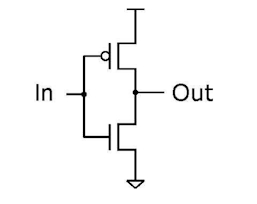
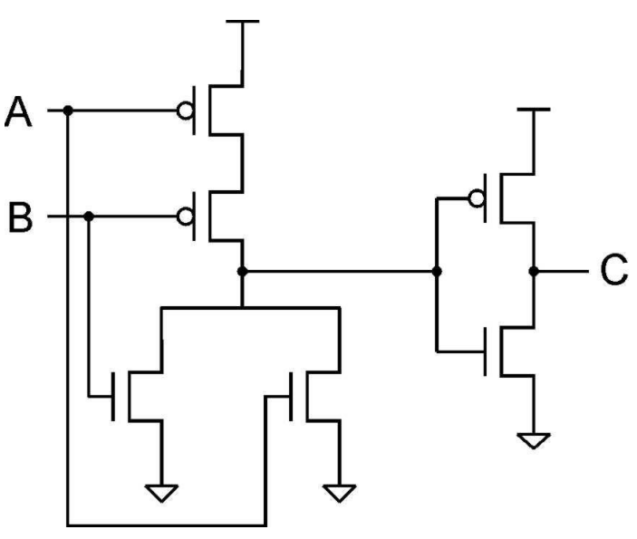
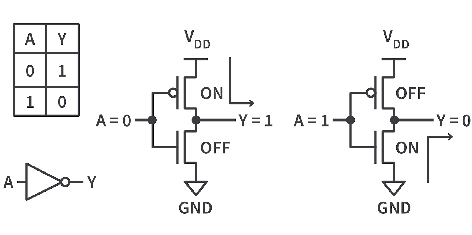
MOSFET - Metal Oxide Semiconductor Field Effect Transistor.

MOSFET is a type of transistor used in electronic circuits for switching and amplification. It consist of metal gate electrode separated from the semiconductor channel by a thin layer of oxide, when voltage is appiled to the gate an electric field is created which controls the flow of current through the channel between the source and drain.

Source is connected to ground.

Drain is connected to load.

Gate is connected to input.


There are two main types of MOSFETs:


N-channel MOSFET (NMOS): In an NMOS transistor, the semiconductor channel is made of n-type material (electron-rich). The gate voltage controls the flow of electrons from the source to the drain. When a positive voltage is applied to the gate with respect to the source, it creates an electric field that attracts electrons, forming a conductive channel between the source and drain, allowing current to flow.


P-channel MOSFET (PMOS): In a PMOS transistor, the semiconductor channel is made of p-type material (hole-rich). The gate voltage controls the flow of holes from the source to the drain. When a negative voltage is applied to the gate with respect to the source, it creates an electric field that attracts holes, forming a conductive channel between the source and drain, allowing current to flow.


Transistor

A transistor is a semiconductor device used to amplify or switch electrical signals and power. It is one of the basic building blocks of modern electronics.

It has three terminals, namely Collector, Base, Emitter.


28 July 2023

D - Flip Flop

The D flip-flop is a two-input flip-flop. The inputs are the data (D) input and a clock (CLK) input. The clock is a timing pulse generated by the equipment to control operations. The D flip-flop is used to store data at a predetermined time and hold it until it is needed.


The D flip-flop has two main inputs:


  • D (Data input): This input controls the data to be stored in the flip-flop. The current value of D is transferred to the output (Q) on the rising edge (or falling edge, depending on the type of DFF) of the clock signal.
  • CLK (Clock input): The clock signal is used to control the timing of the D flip-flop. The output Q is updated based on the value of D at the specific edge of the clock signal.


The D flip-flop has two outputs:


  • Q (Output): Represents the stored data bit. It changes its state based on the input D at the rising (or falling) edge of the clock.
  • Q̅ (Complement output): Also known as the "not Q" or "Q-bar" output, it represents the complement of the Q output.


1. Schematic diagram


2. Logic diagram


2 × 1 MUX

A 2 × 1 multiplexer consists of two inputs IN1 and IN2, one select input SEL and one output OUT.

Logic diagram and Schematic symbol


2x1 mux diagram (2).png


If SEL is 0, then IN1 will be selected.

If SEL is 1, then IN2 will be selected.


D-Algorithm

Inducing the fault in any node and propagating the fault effect from the fault site to the primary output is called D-Algorithm. D-Algorithm...